Electronic Microscopy by Transmission (TEM)


2 Microscopes is available in C2N which are corrected of spherical aberrations. And C2N have an electronic microscope with Focused Ion Beam and some different possibilities of chemical and mechanical thinner..


Microscope JEOL 2200 FS

  • A spherical aberration corrected instruments on condenser lenses provide 1 Angstrom resolution in STEM mode.
  • Ultra high resolution objectif lens provide 1.9 Angstrom resolution in TEM mode.
  • An x ray energy-dispersive spectrometer in the column with omega filter type.
  • CMOS Gatan OneView fast camera.
  • All technic and software solutions to realize 4DSTEM experiments..

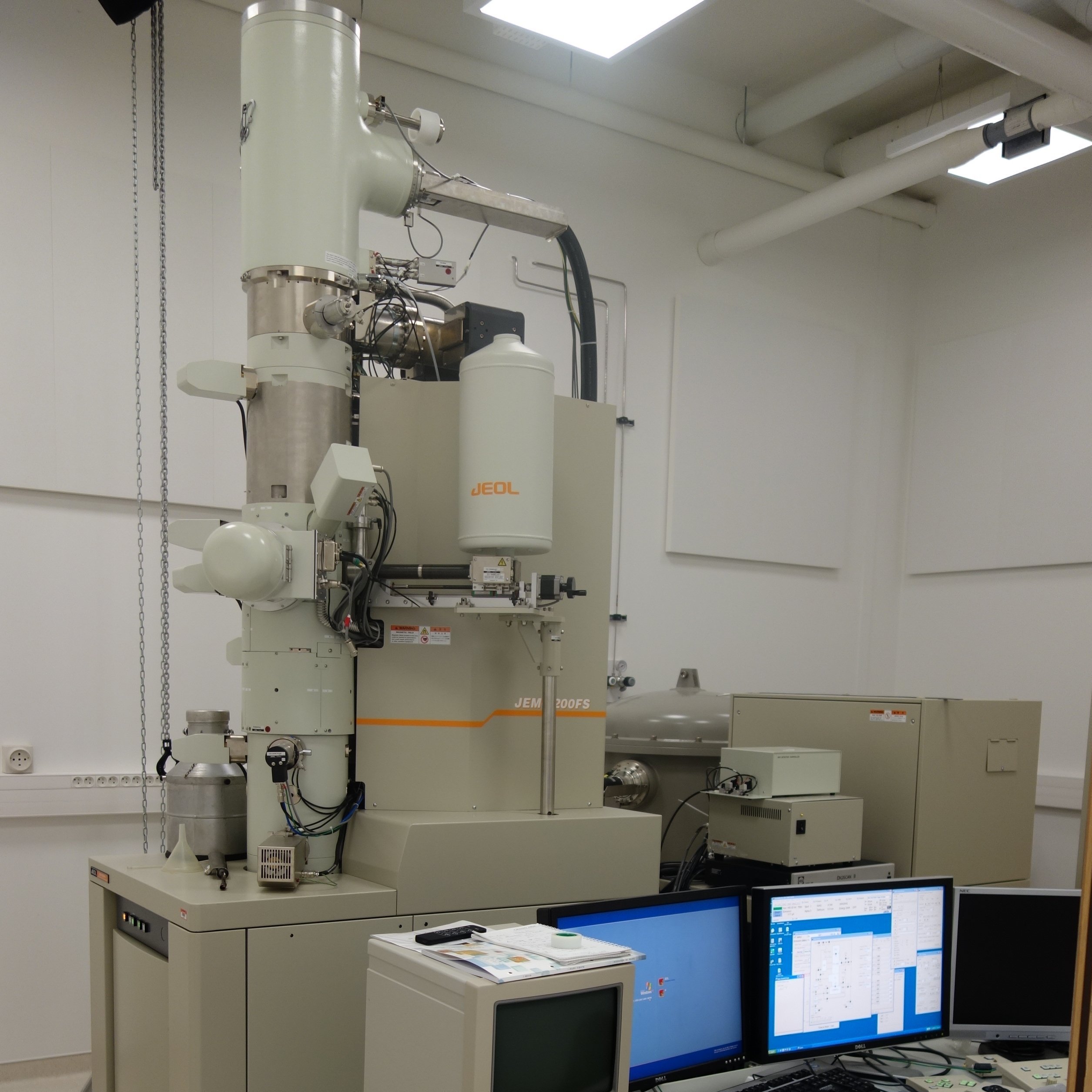
This instrument allow : a high analysis of the interfaces quality, the local structure determination, the local orientation and chemical composition of samples, the study of relaxation modes and the structure resolution. All with a sub-nanometric spatial resolution. Usual technics are conventional imaging, quantitative contrast TEM 2 waves and STEM-HAADF analysis, high resolution imaging, X-ray microanalysis, convergent beam diffraction and 4DSTEM analysis.

C2N is a partner of EQUIPEX TEMPOS.


C2N accommodates and coordinates the NANOTEM platform, composed of a FEI ThermoFisher THEMIS 80-200 keV TEM/STEM with Cs aberration corrector on condenser lens and 4-dial EDX detector, and a FEI ThermoFisher Dual-beam SCIOS focused ion milling system for producing thin TEM slides.


EQUIPEX TEMPOS

NANOTEM Plateform


Microscope FEI ThermoFisher TEM/STEM Titan Themis 200 :

  • XFEG gun with high brilliancy 80-200 keV
  • geometric aberrations corrector on condensor lens which can obtain a 80 picometer spatial resolution.
  • 4 quadrants Chemistem Super-X (EDX) detector system.
  • some STEM BF, ABF et HAADF detectors.
  • S-Twin pole piece with an 2,4 Angstroms resolution
  • TEM CMOS 4k x 4k camera

TEMPOS EQUIPEX

NANOTEM Plateform


FEI ThermoFisher dual-beam SCIOS focused ion milling system microscope

  • UHR NiCol electronic beam
  • Sidewinder 500V-30kV ionic beam
  • Various back scattered and secondary electron detectors : trinity in-lens detector, Everhart-Thornley and ion ICE.
  • Easy-lift in-situ manipulator.
  • Platine et Carbon gaz injector system.
 
C2N also contribute to from TEMPOS EQUIPEX, dedicated at eal-time study of nanocrystal growth with atomic resolution in FEI Titan ETEM 300kV environmental electron microscope establish at the Ecole Polytechnique.


Illustrations :


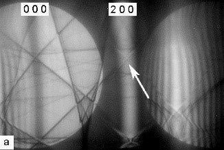
Electronic diffraction imaging with 5 waves convergent beam to determine crystal polarity of GaAs crystal – C2N study.

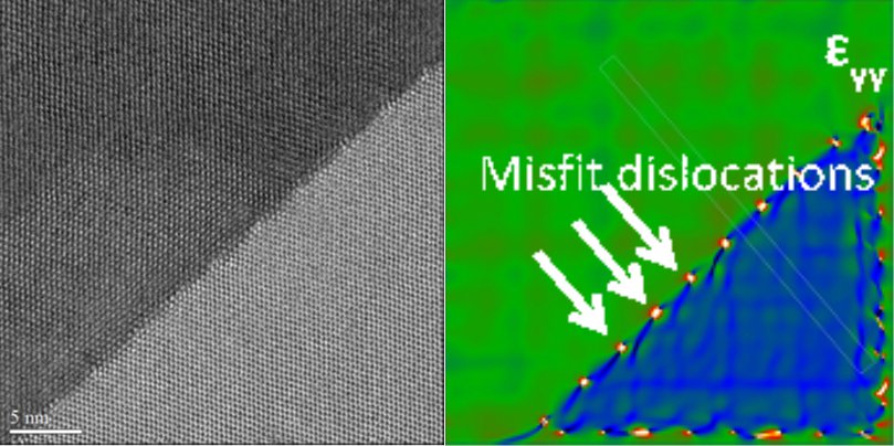
STEM-HAADF imaging of GaSb layer deposit in MBE on Si substrat. Proof of perfect dislocations interface-edge type to accomodate lattice parameter gap. Illustrate the III-V/Si monocrystal growth without threading dislocations - C2N-IES collaboration.

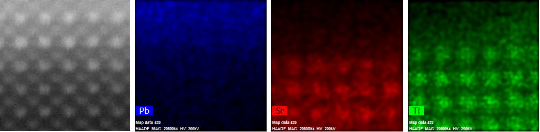
STEM-HAADF imaging et chemical maps by EDX of (Pb,Zr)TiO3/SrTiO3 interface . Illustrate epitaxy obtained by annealing of a sol-gel deposit – C2N-INL collaboration.

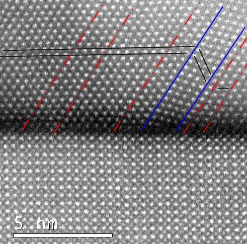
STEM-HAADF imaging of partial dislocations (red) and twins (blue) in InP layer deposit in MBE on SrTiO3 substrat, Illustrate of III-V/oxyde monocrystal growth, to determine epitaxy relationship and characterize the interface – C2N-INL collaboration.
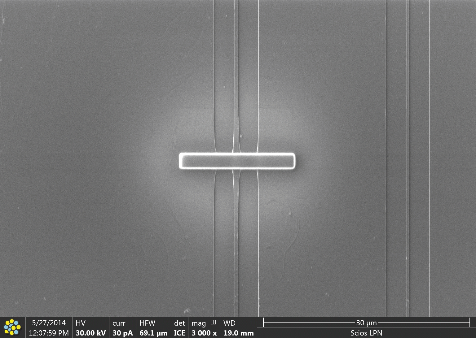