Atomic Force Microscopy (AFM)


Atomic force microscopy is now an essential tool for characterising surfaces at nanometric and atomic scales.  The various AFMs are highly compatible with other surface characterization techniques, like electronic microscopy and Raman spectrometry. The atomic force microscopy provides access for topography to the surface roughness quantification and measurements like height of object or structure which be builded by nanotechnologies.
Differents complementaries modes are possible, at nanometric scales : the nanomanipulation of objects, the magnetic domains mapping (MFM). Electrics modes like local potentiel measurement of surface (KFM) allow to quantifie relative potential of each material on bidimensional stacking materials. The piezoréponse measurement (PFM) allow to read or write piezoelectric domain in plane and out of plane. Local resistivity mapping is possible ( local intensity/voltage measurement).


BRUKER Icon AFM :

  • Cassic modes : Topography, MFM, EFM / KPFM
  • Specific modes  : I/V (contact, peakforce), nanomanipulation, LAO
  • Samples size : from mm to 20 cm
  • Z resolution until 0.03 nm
  • Optic camera resolution : 1 µm

BRUKER DI3100 AFM:

  • Classic modes : Topograpy, MFM, EFM / KPFM
  • Specific modes : nanomanipulation, LAO
  • Samples size : from mm to 20 cm
  • Z resolution : until 0.05 nm
  • Optic camera resolution : 1 µm

BRUKER Multimode Nanoscope III AFM :

  • Classic modes : Topography, MFM, EFM (amplitude)
  • Specific modes : STM, LAO
  • Samples size : from mm to 1.5 cm
  • Z resolution : until 0.03 nm
  • Optic camera resolution : 1 µm

BRUKER Multimode Nanoscope IIIa AFM :

  • Classic modes : Topography, MFM, EFM / KFM (amplitude and phase)
  • Samples size : from mm to 1.5 cm
  • Z resolution : until 0.03 nm
  • Optic camera resolution : 1 µm

Illustrations :


Surface characterization demonstrate by AFM


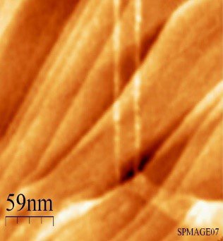
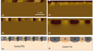
GaAlAs/GaAs Nanofils :
Core-shell structure of GaAs/GaAlAs nanofils in epitaxial layer by MBE,  analysis by AFM in transverse section. We mesure AlGaAs shell thickness.

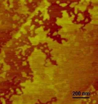
Epitaxial Graphene Layer :
SiC substrat sublimation build some layers. The goal is to control the growth of large (1 µm) Graphene terrace.

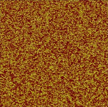
Metal deposit control :
Surface morphology, roughness and thickness of a metallic thin layer by AFM. Rq = 2 nm (picture of 3x3 µm). Process optimisation of metallic deposit of supraconductor NbN very thin (10 nm) film by spraying.


  Magnetic Force Microscopy


Magnetic domains structure of MnAs/GaAs(001) :
MnAs electrodes on GaAs(001) behaves as classic magnetic rungs with a hiigh uniaxial anisotropy in the plane. This promote an open configuration of magnetic domains which was observed by MFM measurement in transversial section of  MnAs/GaAs(001) split layer.


Electric Force Microscopy


III/V layer on Si :
I/V AFM measurements of GaAs nanocrystals on Si substrat and buried nanofils (G. Hallais, Dpt Matériaux).


Nanomanipulation


Nanomanipulation of 2D materials:
Twist angle control in van der Waals heterostructures (R. Ribeiro-Palau, Nanoelectronic Dpt)
.